Last updated 7 January 2009
- "Programming" a PIC in this context refers to storing the program onto a PIC, not generating or writing the program. This process starts with a HEX file, which specifies exactly how the non-volatile memory bits of a PIC are to be set. The process of programming is copying this information from the HEX file into the PIC. There is no way to plug a PIC into a standard computer (PC). A separate piece of hardware, called a programmer is required to connect to an I/O port of a PC on one side and to the PIC on the other side. There are many different PIC programmers available. Most of these use the parallel port, a serial port (COM port), or the USB. The type of programmer, how it connects to the PC, and the various advantages and disadvantages of each are not within the scope of this document. On the PIC side there are two possibilities, socket and in-circuit. A socket programmer provides a way to connect just a bare PIC to the programmer. Since all the connections are built into the programmer, their details are irrelevant to the end user. In-circuit programmers however connect to the PIC while it is connected to the target circuit. Due to variations in the interconnect scheme and the target circuit surrounding the PIC, there is no PIC programmer that works with all possible target circuits or interconnects. The purpose of this document is to help the circuit designer understand the constraints imposed on the circuit by in-circuit programming and to give some guidance on how to design circuits most likely to work with a variety of in-circuit PIC programmers and the Embed Inc PIC programmers in particular.
- PICs are programmed using 5 signals. The data is transferred using a two wire synchronous serial scheme, with the clock always controlled by the programmer. The ICSP signals are:
- Negative power input to the PIC and the zero volts reference for the remaining signals. Voltages of the other signals are implicitly with respect to GND.
- This is the positive power input to the PIC. Some programmers require this to be provided by the circuit (circuit must be at least partially powered up), some programmers expect to drive this line themselves and require the circuit to be off, while others can be configured either way (like the Microchip ICD2). The Embed Inc programmers expect to drive the Vdd line themselves and require the target circuit to be off during programming.
- Programming mode voltage. This must be connected to the MCLR pin, or the Vpp pin of the optional ICSP port available on some large-pincount PICs. To put the PIC into programming mode, this line must be in a specified range that varies from PIC to PIC. For 5V PICs, this is always some amount above Vdd, and can be as high as 13.5V. The 3.3V only PICs like the 18FJ, 24H, and 33F series use a special signature to enter programming mode and Vpp is a digital signal that is either at ground or Vdd. There is no one Vpp voltage that is within the valid Vpp range of all PICs. In fact, the minimum required Vpp level for some PICs can damage other PICs.
- Clock line of the serial data interface. This line swings from GND to Vdd and is always driven by the programmer. Data is transferred on the falling edge.
- Serial data line. The serial interface is bi-directional, so this line can be driven by either the programmer or the PIC depending on the current operation. In either case this line swings from GND to Vdd. A bit is transferred on the falling edge of PGC.
GND
Vdd
Vpp
PGC
PGD
- For many products containing PICs, it is desirable to load a blank PIC on the board during assembly, then program it in-circuit as part of the final production test procedure. This usually reduces cost and allows for a much shorter lead time from new code available until it can be deployed in newly produced units. While the advantages of last minute in-circuit programming are usually compelling, it is not free and ICSP capability must be considered up front when the circuit is designed. It can be difficult and costly to retrofit a circuit for ICSP after other design decisions have already been made. On the other hand, the added cost of ICSP is usually minimal when it is included in the original design requirements.
Here are issues to consider when designing a circuit for ICSP:
- This may sound obvious, but it requires some thought. For low volume products, the cost of an additional connector may be minor, but what connector is appropriate? For high volume designs, the per-unit cost must be kept to a minimum, and some complexity can be pushed onto the test fixture. Here are some suggestions:
- This is a 6 pin "phone" type connector. It's not a great connector but has the primary advantage that it is directly compatible with the Microchip ICD2. Some third party programmers (including some of the Embed Inc programmers) have ICD2 outputs for easy compatibility. This type of connector is a good choice for hobby projects or prototypes where the ICSP connections will be used for debugging or frequent programming during development. For example, this is the connector used on the ReadyBoard-01 and ReadyBoard-02 for the main processor. Due to the way the standard ICD2 cable is wired, the pinout of the target connector must be flipped from the pinout of the same RJ-12 connector built into the ICD2. There ICD2 cable pinout is described in detail in a later section of this document. Another problem with this connector is that the PGC and PGD lines are adjacent on the flat cable, and therefore susceptible to crosstalk. There is more on this also later in this document.
- These type of connectors are cheap, widely available, reliable, and require less board area than a RJ-12 jack. We recommend the keyed version so that the cable can only be plugged in one way. It is not quite as easy to plug and unplug the cable from this connector as for an RJ-12 jack, so this is a good choice for infrequent programming as apposed to active debugging. For example, this is the connector used on the ReadyBoards for the power supply control processor. A 6 pin version of this type of connector can also be used. An extra GND pin added between the PGC and PGD lines greatly reduces crosstalk between these lines, which can be a major problem. The programming output lines of the Embed Inc PIC programmers are available via such a 6 pin header or bare pads (among other options) to facilitate making cables with reduced PGD/PGC crosstalk.
- This is the ultimate in low per-unit cost, but requires a custom fixture to hold the unit during programming. This can be a good choice for high volume designs.
RJ-12 jack
.1 inch header
Pogo pin pads
- The programming algorithms for the 5V PICs require that Vpp (MCLR pin) be raised above Vdd during programming. The requirements range from a few volts above Vdd up to about 13V. This pretty much makes it impossible to have MCLR driven from a regular digital output as these wouldn't tolerate such voltages. Since MCLR is a CMOS input and therefore high impedence, it's usually sufficient to drive it from a digital output thru a resistor. Somewhere in the 20K to 100K ohm range is usually a good value. The low end is limited by the current the digital output can tolerate thru its protection diode when 13V is applied to the other end of the resistor. The high end is limited by the voltage offset caused by the leakage current of the MCLR pin times the resistance, and the additional noise susceptibility on a high impedence node in general.
Another consideration on the resistor size is the output impedence of the programmer's Vpp driver. This is deliberately a minimum value for some programmers to avoid damaging the target circuit, while others may have only passive drive in one direction. For example, the USBProg is voltage-regulated when driving high and 20-30 ohms when driving low. The ProProg also has low impedence when driving high and about 100 ohms when driving low. If in doubt, we recommend 20K ohms series resistance from MCLR to the rest of the circuit on the board. There should be a direct connection from the programmer Vpp line to the MCLR pin.
Another issue is that some PICs can be configured so that MCLR has a internal pullup. Enabling this feature makes designing for ICSP more difficult since a simple series resistor to the rest of the circuit would not work. The resistor and the internal pullup form a voltage divider so the MCLR voltage seen by the PIC when the external circuit is driving it low will be some minimum value. Usually the external resistor would need to be too low to be useful for ICSP to guarantee MCLR is below the maximum threshold for a 0 when driven by the on-board circuit. A separate transistor may be required, or the system designed so that the internal pullup is not needed. This is one of the areas where ICSP will impact the design. Nothing is free.
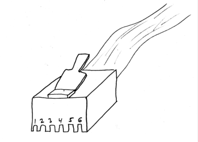
Note that on some PICs, like the 10F20x, the internal pullup is always enabled when the MCLR pin is configured in the MCLR role (as apposed to configured as a normal digital input). There is no universal answer, but this must be carefully considered in the circuit design. The 10F series is already the most challanging to design for ICSP because 5 of only 6 pins will be connected to the programmer.
- Many programmers require control of Vdd during programming. There are three main reasons for this:
- The programmer is a "production" versus "development" programmer according to the Microchip definition, and therefore performs verification at the Vdd voltage limits for that PIC.
- To guarantee the proper voltage for some operations, like bulk erase, which is often specified over a narrower Vdd range than normal device operation. The circuit may provide a valid voltage for the PIC to run, but that voltage may not be valid for a bulk erase and other operations that the programmer must perform.
- To guarantee the correct sequence and sometimes timing of Vdd with respect to Vpp. Some PICs require Vdd raised before Vpp, while others require the reverse. Some PICs also require a minimum time from one to the other.
When the programmer will drive Vdd during programming, the target circuit must be off, or at least the power supply to the PIC must be off. Furthermore the circuit must tolerate the PIC Vdd pin driven up to the PIC's maximum Vdd spec. This is usually 5.5V, and may be several volts higher than the circuit normally operates at or is designed to run at.
Even if the circuit can withstand 5.5V power, it must not draw more current than the programmer can supply. Specifications for programmers vary widely. The EasyProg can only supply 20mA safely, the USBProg and LProg 100mA, and the ProProg 250mA with the supplied wall wart and 500mA with a fixed input supply.
Beware that some linear regulators, like common 7805 for example, can be damaged by raising their outputs above their inputs. A diode from the regulator output to its input my be required.
In some cases it will be necessary to split the power supply of the circuit so that the PIC is powered from a separate segment. Each segment may be driven thru a diode from a master supply. This prevents power on one segment from driving the others, but also presents another problem of the voltage drops accross the diodes. Sometimes it is sufficient to make the master supply 600-700mV higher to compensate for the diode drops. Sometimes the master supply has a voltage feedback path accessible to the circuit. In that case the feedback can be taken from the output of one of the diodes. The voltage of that power segment will be well regulated, with the voltage of the other segments being within a few 100mV because the diode drops will match reasonably well. These are only some ideas. There is no universal answer and each case must be carefully considered with all the issues in mind.
- These are digital signals and will always be driven within the range of GND to Vdd at the time, although Vdd may be higher than normal when PGC and PGD are driven. The drive impedence of the programmer on these lines must also be considered, since this forms a voltage divider with any in-circuit impedence tied to these pins. The EasyProg has 2K ohm drive impedence on both lines, the USBProg 150 ohms, the LProg 200 ohms, and the ProProg has 1K ohm drive impedence on PGD and 270 ohms on PGC.
On large PICs with many pins, it may be appropriate to dedicate the PGD and PGC pins for ICSP. In that case these pins should be configured as outputs and driven low or high during normal operation. They should not be left as floating inputs. In other cases it may be sufficient to put a resistor between these PIC pins and the rest of the circuit. This was discussed in detail for Vpp (above).
- The PIC PGM pin is used to enable low voltage programming on some PICs. Even though this is not one of the programming lines and is not connected to the programmer, it should be held low during programming. According to the documentation the PGM input should not matter during high voltage programming, but we have seen cases where it does anyway. A 100K ohm resistor to ground is a simple fix in most cases.
Provide a connection
Allow for high voltage on Vpp
Consider Vdd driven externally
Consider PGC and PGD driven externally
PGM should be low during programming
- While this is really another circuit constraint, this issue is so unintuitive, little known, poorly documented, but serious that it deserves its own section.
The standard Microchip cable unfortunately puts PGD and PGC on adjacent lines. Since this is a flat cable, this can and does lead to crosstalk between the two in some cases. For writing to the target, the programmer drives both lines. In that case a little low pass filtering can be applied by the programmer to soften the edges and reduce the coupled amplitude on one line from an edge on the other.
However, there is a case that must be addressed by the target circuit. The PGD line is bidirectional, meaning it is sometimes driven by the target PIC. In that case PGD is just a normal digital output on the PIC. These are designed to drive from one state to the other as quickly as possible. Such an edge produced on PGD by the target PIC can couple onto the PGC line when using the standard cable supplied with an ICD2, or any other cable where PGC and PGD are adjacent. The target PIC then sees a PGC (clock) pulse that the programmer didn't produce and the serial communication gets out of sync. The net result is that programming appears to be flaky or not work at all.
This entire effect can happen within the time for the PGD edge to propagate from the target PIC, thru the cable to the programmer, and back thru the cable to the target circuit. This means that this problem can not be solved at the programmer end of the cable. No amount of clever circuitry at the programmer can make this issue go away. It must be dealt with at the target circuit.
This issue is particularly important for dsPICs since they are faster and therefore have stronger digital output drivers and faster edges that couple better between signals. Although somewhat less severe, we have observed this issue on programming 18F PICs. We don't recommend assuming this won't happen on 16F or other PICs. We're not sure that it doesn't, and ignoring it would essentially be relying on a maximum digital output edge slope. This could easily change between production lots, over temperature, or as new fab processes are brought on line.
We recommend filtering the PGD output from the target PIC by adding 100 ohms in series followed by 47-100pF to ground. This limits the slope of edges and attenuates the high frequecy components that can couple from PGD to PGC. We also recommend adding the same capacitance to ground to the PGC line close to where it enters the target board by the programming connector. This reduces the impedence of the PGC line at high frequencies, which reduces its susceptibility to crosstalk.
We had previously recommended 22pF for both capacitors instead of 47-100pF, but have meanwhile found cases where even 22pF was insufficient. We feel that 47-100pF provides sufficient margin but is still below the level where it could interfere with the normal operation of the lines.
For example, the USBProg has 150 ohm output impedence on both lines. 150 ohms times 100pF is a time constant of 15nS, making the 90% settling time about 45nS. This is small compared to the minimum 500nS time from data to clock edges used by that programmer. Other Embed Inc programmers have higher impedences and therefore longer time constants, but also longer data setup times to compensate. All the Embed Inc programmers will work with a additional 100pF load on the PGC and PGD lines.
- We define the pins of the connectors on an ICD2 cable as shown in this drawing:
Signal ICD2 end pin Target end pin Vpp 6 1 Vdd 5 2 GND 4 3 PGD 3 4 PGC 2 5 not connected 1 6


http://www.embedinc.com/picprg/icsp.htm
ReplyDelete